TSMC Is Building an Advanced Chip Packaging Plant in Arizona by 2029
TSMC announced it will build an advanced chip packaging facility in Arizona, targeting completion by 2029. This is not just another fab — advanced packaging is the technology that stacks multiple chips together into a single unit, and it is increasingly critical for AI hardware. The US is getting a piece of it.
What's Actually Happening
Advanced chip packaging — technologies like CoWoS and SoIC that TSMC pioneered — allows chipmakers to combine multiple dies into one package, dramatically improving performance and power efficiency. Nvidia's H100 and H200 GPUs rely on this kind of packaging. Until now, most of that capacity has been concentrated in Taiwan.
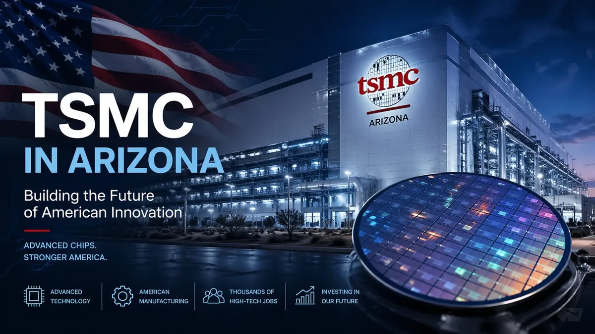
The Arizona facility will extend TSMC's US footprint beyond the two fabs already under construction there. It signals that TSMC is committing to a more complete semiconductor supply chain on American soil, not just front-end wafer fabrication.
Why It Matters
The chip packaging bottleneck has been one of the quietest constraints on AI hardware supply. When Nvidia's GPUs were on long waitlists, part of the reason was packaging capacity — not just wafer production. Moving this capability to Arizona reduces single-country dependency and puts critical AI infrastructure closer to TSMC's largest customers.
For US semiconductor policy, this is a significant win. The CHIPS Act has already incentivized TSMC's wafer fabs. Adding packaging capability completes more of the value chain domestically. Related: Google's TPU chips are another piece of the US effort to build independent AI hardware capacity.
My Take
TSMC expanding to packaging in Arizona is bigger news than it sounds. Packaging has been the hidden chokepoint in the AI hardware supply chain — everyone focused on fab capacity while packaging bottlenecks quietly throttled GPU supply. A US-based CoWoS facility means Nvidia, AMD, and Apple can get packaging done without shipping wafers back to Taiwan.
The 2029 timeline is realistic but not fast. AI hardware demand is being measured in 2025 and 2026 terms. This facility helps 2029 and beyond — it does not solve today's shortages.
Frequently Asked Questions
What is advanced chip packaging? Technology that combines multiple semiconductor dies into a single package, enabling chips to communicate faster and more efficiently than if they were on separate boards.
Why does this matter for AI? Modern AI chips like Nvidia's H100 depend on advanced packaging to achieve their performance. Packaging capacity is a genuine supply constraint.
Where is TSMC's existing US presence? TSMC is building two wafer fabs in Phoenix, Arizona, with the first targeting N4 process technology.