TSMC's AI Chip Packaging Is Growing at 80% Per Year — And Nvidia Has Most of It Locked Up
The most critical bottleneck in the AI revolution isn't models or data — it's chip packaging. TSMC just revealed that its most advanced packaging technology, CoWoS (Chip on Wafer on Substrate), is growing at an astonishing 80% compound annual growth rate. And NVIDIA has locked up the lion's share of that capacity for years to come.
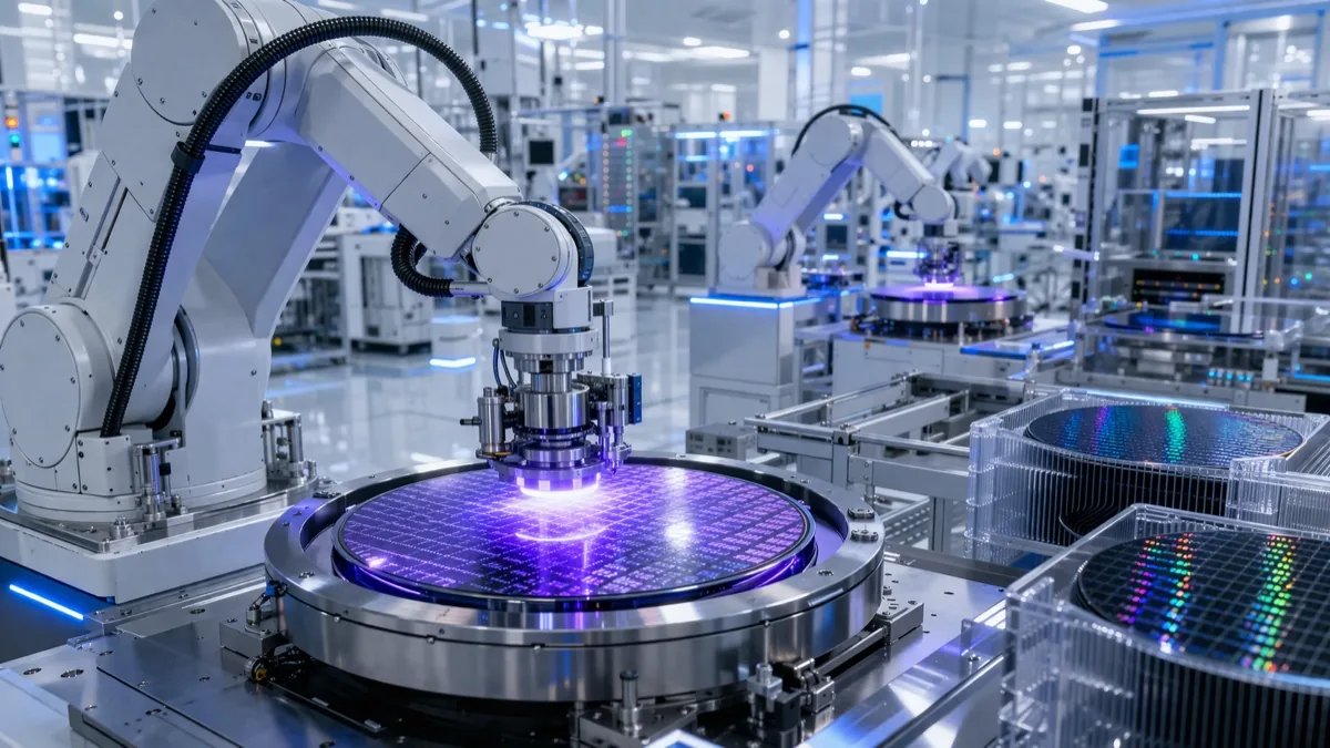
What Is CoWoS and Why Does It Matter?
Modern AI chips like NVIDIA's H100, H200, and Blackwell aren't just individual processors — they're complex assemblies of multiple chips, memory stacks, and interconnects packaged together on a single substrate. CoWoS is the technology that makes this possible, allowing TSMC to stack computing power far more densely than traditional packaging methods.
Without advanced packaging, even the most brilliantly designed AI chip can't reach its full potential. It's the bridge between chip design and real-world performance, and right now, TSMC is the only company that can do it at the scale the AI industry demands.
NVIDIA's Packaging Lock
NVIDIA has reportedly reserved over 50% of TSMC's projected CoWoS capacity for 2026-2027, with some reports suggesting the reservation extends even further. This means competitors like AMD, Google (for its TPU chips), and emerging AI chip startups face significant constraints in accessing the packaging capacity they need.
This isn't just a supply chain detail — it's a strategic moat. By locking up advanced packaging capacity, NVIDIA ensures it can ship more AI chips than anyone else, regardless of whether competitors design equally capable silicon. The enterprise AI spending shift means demand for these chips is only accelerating.
TSMC's Expansion Plans
TSMC isn't standing still. The company aims to produce 130,000 CoWoS wafers per month by late 2026 — nearly quadrupling its output from late 2024 levels. This massive ramp-up reflects the extraordinary demand from AI companies.
To handle the surge, TSMC has also begun outsourcing some packaging steps to ASE, the world's largest outsourced semiconductor assembly and test company. ASE expects its advanced packaging sales to double in 2026.
The U.S. Expansion Factor
TSMC is also expanding its advanced packaging capabilities in the United States, part of a broader effort to diversify production beyond Taiwan. This has geopolitical implications, as the concentration of advanced chip packaging in Taiwan has been identified as a strategic vulnerability by multiple governments.
What This Means for AI
The 80% CAGR in advanced packaging tells us something important: the AI hardware boom is far from over. Companies are willing to commit years of capacity in advance because they believe AI demand will only grow. For investors, enterprise customers, and tech companies alike, the chip packaging supply chain has become one of the most important factors determining who can build and deploy AI at scale.
Frequently Asked Questions
What is TSMC CoWoS?
CoWoS (Chip on Wafer on Substrate) is TSMC's most advanced chip packaging technology. It allows multiple chips, memory stacks, and interconnects to be assembled on a single substrate, enabling the dense computing power needed for AI chips like NVIDIA's Blackwell and H200.
Why is CoWoS growing at 80% per year?
Demand for AI chips is driving explosive growth in advanced packaging. AI processors require increasingly complex multi-chip assemblies, and CoWoS is the only technology that can deliver this at the scale the industry needs.
How much CoWoS capacity does Nvidia have?
Nvidia has reserved over 50% of TSMC's projected CoWoS capacity for 2026-2027, effectively creating a strategic moat that limits competitors' ability to ship advanced AI chips at comparable volumes.
Can other companies access CoWoS?
Yes, but capacity is limited. AMD, Google, and AI chip startups face constraints. TSMC is quadrupling output to 130,000 wafers/month by late 2026 and outsourcing some steps to ASE to meet demand.